<<- Back ^- Intro -^ Forward ->>
Chapter 2: VCA
THE VCA
VCA Circuit
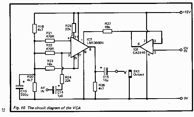
The circuit diagram of the VCA appears in Figure 10. This is based on one of the transconductance amplifiers in an LM1360ON or LM1370ON (IC7), and unlike the previous circuits this one operates from a single 12 volt positive supply rather than dual balanced 12 volt supplies. R19, R20, and C13 are used to provide a centre tap on the supply for biasing purposes. The VCA is an entirely conventional type which makes use of the linearising diodes at the input of the amplifier. A bias current is fed to these by R25, and this gives improved distortion performance from the circuit. The output impedance of the transconductance amplifier is quite high, but IC-7 includes an output buffer amplifier in the form of a Darlington Pair emitter follower stage, and this provides ,'the circuit as a whole with a low output impedance. R26 is the 'discrete load resistor for this stage.
R27 is included in series with the amplifier bias input of 1C7 to de a conversion from current to voltage control. The VCA has a linear rather than a logarithmic control characteristic, but this is perfectly satisfactory and there is no need to add a logarithmic converter ahead of the control input. What is needed here is a buffer amplifier to provide a very high input impedance at the control input of the unit. 'This is necessary because of the very high output impedance of the envelope generator circuit.
VCA Components (Fig. 10)
Resistors (all 1/4 watt 5%)
R19,20,26 4k7
R21,22 47OR
R23,27 18k
R24,25 22k

Capacitors
C13 220,gF 10V radial electrolytic
C14 -1uF 63V radial electrolytic
C15 lOgF25Vradialelectrolytic

Semiconductors
IC7 LM1360ONorLM1370ON
IC8 CA3140

Miscellaneous
SKI Standard jack socket
Printed circuit board
Wire, solder, etc.
