<<- Back ^- Intro -^ Forward ->>
Chapter 2: VCF
THE VCF
VCF
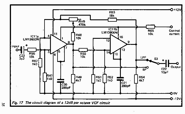
Figure 17 shows the circuit diagram of the VCF. Like the VCA, this should have its control input driven by way of the logarithmic to linear converter (Figure 7).
Also in common with the VCA, this circuit is based on the two transconductance amplifiers and buffer stages in an LN1360ON or LM1370ON. The circuit consists of two single stage lowpass filters connected in series. In the first of these IC11a acts as a voltage controlled resistor while C20 is the filter capacitor, and in the second 1C11b acts as the voltage controlled resistor while C21 is the filter capacitor. Being a two stage filter the attenuation rate is 12dB per octave.
Feedback via R48 and R53 -RV9 provides a bandpass response at the output of 1C11a, and also gives variable resonance. The resonance control can be used to both give a peak in the response just below the cutoff frequency of the filter in the lowpass mode, or to narrow the response in the bandpass mode. S3 is used to select the required type of filtering. The filter has a wide operating frequency range, and its cutoff frequency can in fact be varied over the full audio range.
VCF Components (Fig. 17)
Resistors (all 1/4 watt 5%)
R47,51,52,57	lk
R48,53	18k
R49,54	4k7
R50,55	10k
R56	15k

Potentiometers
RV9	470k linear

Capacitors
C20,21	390F ceramic plate
C22	10uF 25V radial electrolytic
C23	2u2 63V radial electrolytic

Semiconductors
IC11	LM13600N or LM13700N

Miscellaneous -
Printed circuit board
Control knob, wire, solder, etc.
