<<- Back ^- Intro -^ Forward ->>
Chapter 2: VCO
THE VOLTAGE CONTROLLED OSCILLATOR
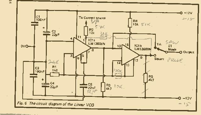
The basis of any analogue synthesizer is its VCO (or VCOs), and this is the module that we will consider first. The circuit diagram of the VCO appears in Figure 6.
IC1 is an LM13600N dual transconductance amplifier (or the virtually identical LM13700N), and devices of this type are much used in electronic music. What makes transconductance amplifiers so useful is their ability to operate as a sort of voltage controlled resistance, a feature which makes them suitable for use in VC0s, VCAs, VCFs, and certain types of modulator circuit. In this case the two amplifiers are connected in an arrangement that is similar to a conventional triangular-square wave oscillator using a Miller Integrator and a Schmitt Trigger. IC1a operates as the integrator while IC1b is the trigger circuit. The triangular waveform is available, from IC1a and IC1b provides the square wave output.
Although this circuit has been described as a VCO, this is not really a very accurate description in that transconductance amplifiers' are current rather than voltage operated. It is therefore the control current fed to the amplifier bias input (pin 1) which controls the operating. frequency, and not the voltage applied here. In order to obtain voltage operation it is merely necessary to add a resistor in series with the bias input, as the current flow is then roughly proportional to the applied voltage.
This is not a suitable solution in this case as it would result in a 'VCO having a reasonably linear voltage-frequency characteristic, whereas what is needed is a type having a logarithmic control law. In other words, we require a circuit where the pitch is raised in octave steps by control voltages of 1 volt, 2 volts, 3 volts, 4 volts, etc. With a linear control law the control voltage must be doubled in order to provided each octave increment. Designing a VCO which has a logarithmic control law would be a difficult task, and the normal approach is to use a linear VCO fed from a logarithmic to linear converter. While it might seem easier to just design the keyboard circuit to suit a linear VCO and eliminate the need for what is a difficult form of voltage conversion, this is not really the case. The logarithmic law enables a very simple keyboard circuit based on readily available components to be adopted, whereas with a linear characteristic it would probably be impossible to obtain suitable precision resistors. This would make it necessary to tune each note of the keyboard individually. It would also make digital control of the circuit a more difficult proposition.
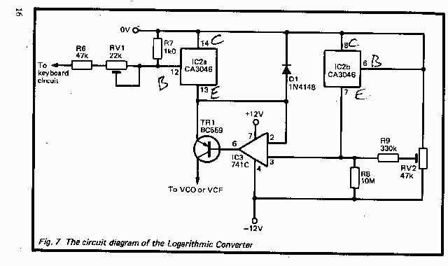
The circuit diagram of suitable logarithmic to linear converter appears in Figure 7. This is also a voltage to current converter, and the VCO remains a current rather than a true voltage controlled type despite the inclusion of series resistor R2 at its input. R2 is only a current limiting resistor to protect IC1a against an excessive input current, and it plays no active role in the VCO.
This converter circuit, in common with most other types of logarithmic amplifier, relies for its operation on the fact that the current through a forward biased silicon diode rises exponentially with linear increments [it!] the input voltage. Although this characteristic is only maintained over certain limits, in this application there is no need to exceed these limits as only a modest ,range of output currents is involved (no more than a range of about 100 to 1). What does complicate things is that the voltage across a forward biased silicon diode varies significantly with changes in temperature, and diodes are often used as electronic temperature sensors. The circuit must therefore include temperature compensation to avoid the need for very frequent readjustment to correct tuning drift.
Having tried a variety of configurations, this one seems to give reasonably accurate and stable results without the need for any “difficult to obtain” components. IC2 is a CA3046 transistor array, which consists of three individual transistors plus two others connected as a long-tailed pair (i.e. having their emitters connected together). In this circuit only two of the individual transistors are used, and no connections are made to the other devices. IC2a operates as the converter, while IC2b provides a degree of temperature compensation. The point of using a transistor array to provide these two devices is that this ensures excellent thermal contact between the two, and consequently gives instant and accurate temperature compensation. The alternative of using two ordinary silicon NPN transistors with their cases glued together seems to work reasonably well, but the additional expense of using a transistor array is probably justified.
The input voltage range is far too large to directly drive IC2a, and a potential divider to provide a suitable degree of attenuation is therefore included at the input of the circuit. RV1 is adjusted to give the required 1 volt per octave characteristic. RV2 is the frequency control, and this enables the output current of the circuit to be adjusted. In practice this acts as the tuning control, and it is adjusted to give the required pitch range from the VCO. It provides a large control range, and enables the pitch range to be shifted over at least three octaves. A more detailed description of setting up RV1 and RV2 will be provided later.
VCO Components (Fig. 6)
Resistors (all 1/4 watt 5%)
Rl lk
R2 10k
R3,5 4k7
R4 15k

Capacitors
Cl,3 100nF ceramic
C2,4 22uF 25V radial electrolytic
C5 22nF miniature polyester

Semiconductors
IC1 LM13600NorLM13700N

Miscellaneous
S1 SPDT miniature toggle switch
Printed circuit board, wire, etc.
Log-Lin Converter Components (Fig. 7)
Resistors (all 1/4 watt 5%)
R6 47k
R7 lk
RS 10M
R9 330k

Potentiometers
RV1 22k miniature horizontal preset
RV2 47k miniature horizontal preset

Semiconductors
IC2 CA3046
1C3 741C
TR1 BC559
DI 1N4148

