E-Music DIY Reference Archive
LM13600/LM13700
A Short Discussion of the
Operational Transconductance Amplifier (OTA)
In the late sixties, RCA, then one of the major leaders in linear semiconductors, came out with the Operational Transconductance Amplifier, hereafter called OTA. The name means essentially a controllable resistance amplifier. The control input is a current. Like an operational amplifier, there are differential inputs. These inputs are used to modulate the control current. Unlike an op amp, the output of the OTA is a current! Unlike an op amp, there is not a single resistor in the OTA circuit.
I first learned of the OTA in the late sixties from my then employer, Dr. Robert A. Moog, whom a few of you may have heard of. Bob was quite enamoured of the CA3080, but I can’t recall any Moog product during my tenure that ever used it. (Note, I worked for Moog during the modular synth days, before !MiniMoog).
It’s All Done With Mirrors
To understand the OTA, you have to know what a current mirror is. The current mirror was a natural development of integrated circuit op amps in which transistors could be made that were inherently matched. The originator of the OTA, RCA was absorbed by Intersil, which was absorbed by GE, which was absorbed by Harris. Harris still makes the original line of RCA linears, including the CA3080A. The figures that accompany this discussion were cut from .pdf files downloaded from harris.com, and national.com (LM13600) and converted to .GIF files. Specifically, all but the LM13600 figure were cut from Harris Ap Note AN6668.1 which Harris has available as AN6668.pdf. I will refer to the figure numbers that appear on the figures.
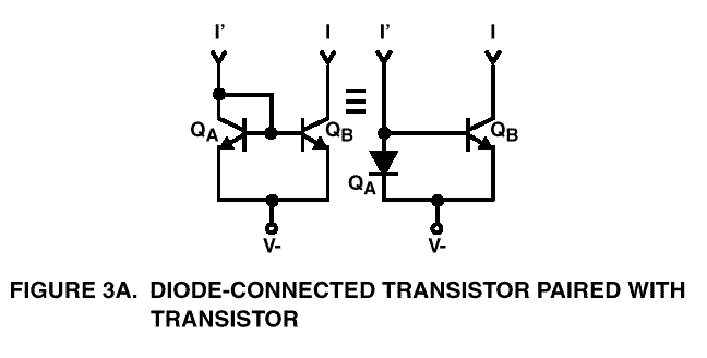
Figure 3A shows a simple current mirror. Let us assume that V- is connected to ground, and that a resistor is connected from +12 to the collector of QA. The collector of QA is connected to the base, so that there is just a diode drop from collector to emitter. The base voltage adjusts itself so that the sum of the base current and the collector current (beta times the base) is equal to the current defined by the resistor. Let us assume that the diode drop is .6 volts. Thus, the voltage across the resistor is about 11.4 volts, and we can select the value of resistor to give us whatever current we like. Since the transistors are monolithic and matched, whatever collector current VBE of QA defines, the same collector current will flow in QB, which sees the same VBE. Since transistor QA acts like a diode, it is typically shown as a diode, as the right side of Figure 3A. shows.
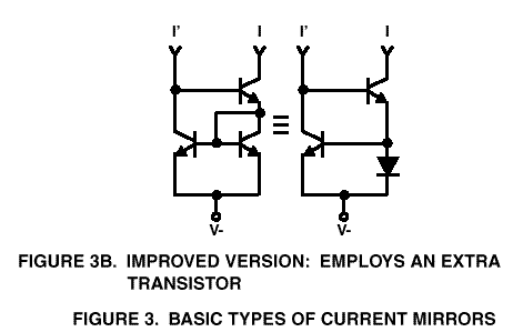
Thus, for the current mirror, current is ‘pushed’ from above (I called it ‘blown’) into the diode, and a very nearly equal current is “pulled” to a low voltage, (I call it ‘sucked’). The current I’ is slightly larger than I since it must also provide base current for both transistors. If beta were 100, one part in 100 would go to each base for an error of about 2%. The accuracy of the mirror can be enhanced significantly by using a more complex mirror, which uses a third transistor. The math for the improved mirror appears in an early RCA linear application book, which I can’t locate for the moment. The improved mirror is shown in Figure 3B. Most monolithic current mirrors use the improved circuit. To summarize, we ‘blow’ into an NPN current mirror from above, and the output sucks an equal current from below. Note, no resistors are required to make a current mirror. By using PNP transistors, we can make a current mirror in which we ‘suck’ current from below and the mirror ‘blows’ an equal current from above. We are now ready to look at the OTA.
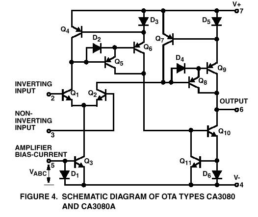
Figure 4. shows a schematic of a CA3080-style OTA. Note that all diodes shown are really diode connected transistors as in Fig. 3A. Note also that the two PNP mirrors are somewhat more complex than the NPN mirrors. This is because it is more difficult to make high gain PNP transistors on the same substrate with NPN, and a Darlington PNP is required. Again, note that no resistors are required.
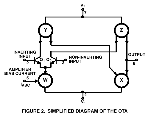
If we now redraw the circuit replacing the mirrors by symbols to represent mirrors, it is relatively easy to see how the OTA works. Figure 2 shows this simplified schematic.
A current IABC is blown into pin 5, and is sucked via mirror W from the input differential pair. Let us suppose for the moment that the input pair are perfectly matched and connected to a voltage midway between V+ and V-. Let the supply voltages be +12 and –12. The current defined by IABC is now divided equally between Q1 and Q2. As we will see shortly, the output of the amplifier is a current. To develop a voltage let us assume that there is a 5K resistor to ground on the output. Assume that the amplifier bias current, I, is 2 ma. Half the current I, 1 ma., is sucked via Q1 from PNP current mirror Y whose output blows an equal current into NPN current mirror X, which sucks an equal current from the output. Half the current I, 1 ma., is sucked via Q2 from PNP current mirror Z, which blows an equal current into the output. Thus, current mirror X is sucking 1 ma, and current mirror Z is blowing 1 ma., and the net current into the output is zero. The voltage at the output is zero.
If we apply an unbalanced drive to the input pair, all of the current will either go through Q1 or Q2, depending on the polarity on the inputs. The output in this case will be either 2ma blown into 5K (+10) or 2ma sucked from the 5K or –10 volts. Any injected current can be turned into alternating + and - currents that are equal and converted to equal + and – voltages. If instead of a resistor, we run the current to the summing node of an op amp connected as an integrator (cap from output to minus), the output of the op amp will ramp up and down with equal slopes, and we can make a current controlled triangle/square wave oscillator. Since it acts as a variable resistance, the OTA is potentially very useful for voltage controlled oscillator, amplifier and filter applications.
But there is a fly in the ointment. The very first current mirror, labeled W in Figure 2., is of questionable utility. It requires that we blow the bias current IABC into the chip, using a PNP transistor current source. How much more convenient if we could directly suck the bias current through the input pair with an NPN transistor.
A case could be made for supplying IABC from above. It may not be easy to operate an NPN current sink on the negative rail with the base just a diode drop above. But there is no reason why you have to do so. A virtue of the current mirror is its voltage compliance. It is able to work with a large VCE voltage or a small VCE voltage with equal ease. So in fact, an NPN sink could be biased to operate less than two volts below common, the reference to the differential inputs.
There is an unfortunate irony in this choice by the designers to employ the input current mirror. The CA3080 uses an 8-pin package. Two pins are unused! All they had to do was to bring out the common emitters of the input transistor pair to one of the unused pins. If pin 5 were then connected to pin 4, the negative rail, then the input current mirror would be open circuited and you would be free to suck, via an NPN, the current through the input pair, if you so chose. With four current mirrors, the CA3080 is useful. With only three mirrors, or a pin brought out to bypass the first mirror, the chip would be even more useful. When RCA brought out the CA13600 (years ago), I read an article in one of the design magazines about it. To my surprise and disappointment, the CA13600 contained the same blunder of one mirror too many. The engineer who wrote the article and had a hand in the design of the chip obvious wasn’t an analog synth guy. I called him on the phone and talked briefly with him. He didn’t know what I was talking about.
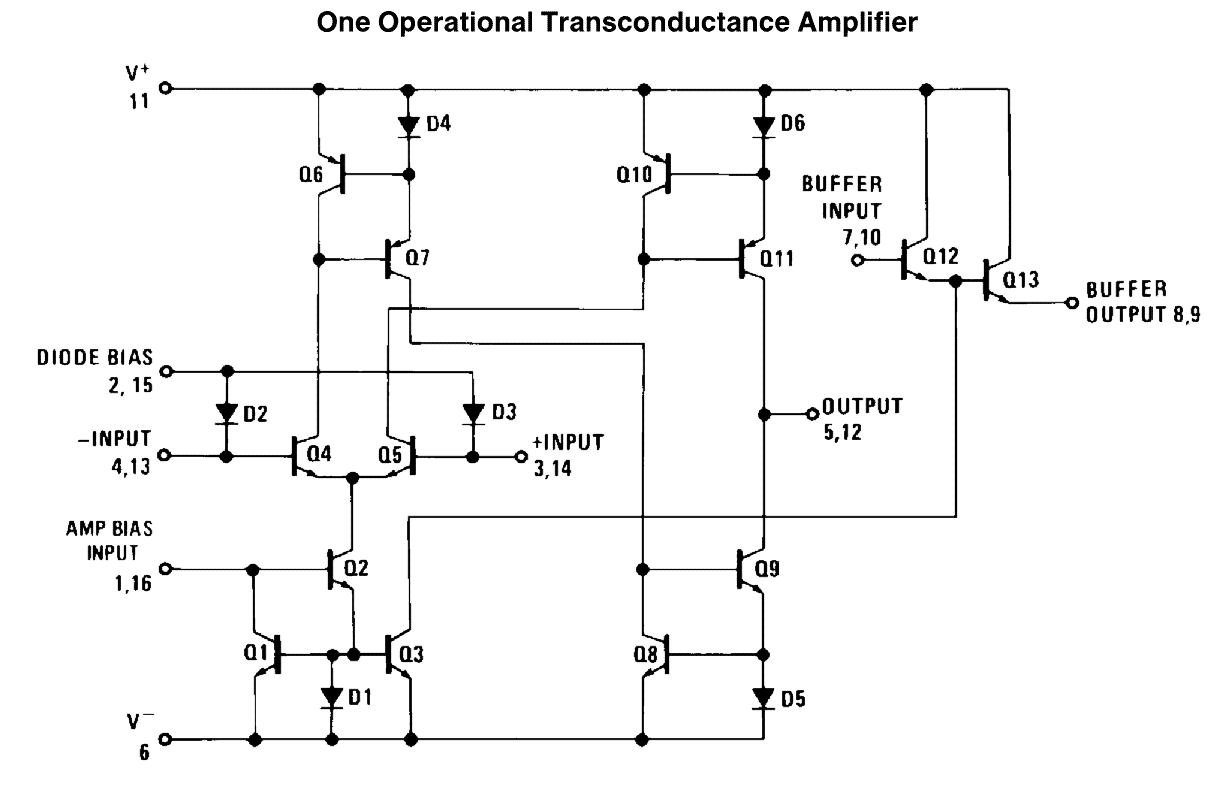
One shortcoming of the original OTA is that in order to avoid serious distortion, the audio signal applied to the differential inputs must be kept very small. The CA13600 addressed this problem and added what it calls linearizing diodes, which permits the output to remain linear with increasing input amplitude. A 10 dB signal to noise improvement is claimed. The CA13600 also provides Darlington buffer followers. The upper limit of IABC is 2 ma. A dynamic range of six decades of gm control is claimed, however. To achieve this range, extremely low IABC currents are required. The bias for the buffers is another current mirror output coming off the input mirror, so that the buffers have an input impedance that matches the bias current magnitude. Apparently this isn’t optimal for audio circuits. Accordingly, the CA13700 is the same circuit as the CA13600 with the exception that the output buffer impedance is independent of the bias current. A schematic for an OTA on the CA13600 is included. The Darlington in the CA13700 (LM13700) has no connection to the input current mirror as the 13600 does.
It is unfortunate that there are so relatively few of us that we can’t easily “roll our own” chips. One of my firsts would be a three-ball OTA, that is, an OTA without the first current mirror. On the other hand, it is truly remarkable that you cannot buy a three-pin NPN current mirror (for $.49) and a 3-pin PNP current mirror ($.79) in a plastic TO-92 package. I REALLY miss the lack of a good, cheap PNP mirror. With an 8-pin package, you could make mirrors with six identical outputs. With a 14-pin package, you could have four independent mirrors. The design of the chip is trivial. It is simply the metalization layer of a matrix of transistor chips. A mix of PNP and NPN mirrors in the same package is not a viable choice. Excellent PNP transistors can be made easily, provided there is no need to make NPN transistors on the same chip.
For those of you who are new at this, I hope that this discussion has shed some light on the CA3080 OTA and its congenital deformity (the extra ball).
It is highly recommended that you visit the harris.com site and download spec sheets and ap notes for the CA3080 if you don’t have them.
Eugene M. Zumchak
Zumchak@cerg.com
February 1999
